Thursday, October 25, 2012

DipTrace 2.3 | 121 MB

DipTrace 2.3

DipTrace 2.3 | 121 MB

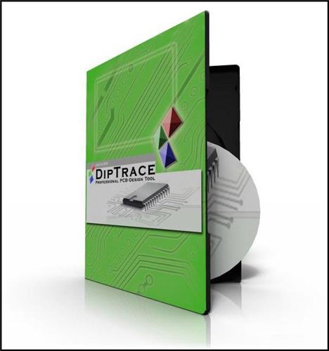
DipTrace is an advanced PCB design software application that consists of 4 modules: PCB Layout with high-class auto-router and 3D PCB Preview, Schematic Capture, Component and Pattern Editors that allow you to design your own component libraries. DipTrace is a useful pattern editor, component editor and much more.


Besides being very simple to learn, this software has a very intuitive user interface and many innovative features. For instance, a schematic can be converted to a PCB with one mouse click. Advanced manual placement and auto-placement features allow to get acceptable placement in several minutes.

The board designer can instantly renew the PCB from an updated version of schematic and keep all previous work without changes. PCB and Schematic can be compared at any design stage to ensure they are identical. Hierarchical and multi-sheet schematics are supported.

DipTrace has a powerful automatic router. It can route a single layer and multilayer circuit boards, and there is an option to autoroute a single layer board with jumper wires, if required.

DipTrace also provides you with external autorouter support. Smart manual routing tools allow users to finalize the design and to get the results they want in a blink of an eye. Accurate shape-based copper pour system with different possible fill types and thermals is available.

Other important features are Electrical Rule Check (ERC), Design Rule Check (DRC) and Net Connectivity Check - the functions that check connections in Schematic by different rules (pin type, short circuit, etc.), the clearance between layout objects, which ensures board accuracy, and connectivity of all nets not depending on how they are connected (with traces, thermals or shapes).

DipTrace modules allow you to exchange schematics, layouts and libraries with other EDA and CAD packages. DipTrace Schematic Capture and PCB Layout also support popular netlist formats and spice. Output formats are DXF, Gerber, Drill and G-code. Standard libraries include 100.000+ components.

Here are some key features of "DipTrace":

· Easy to learn user interface
· To design a schematic, simply select and place components onto your document and connect them together using the wire and bus tools. Multisheet design is supported. Then select the menu option 'Switch to Board' to convert the schematic to PCB. Layout can be updated from Schematic in a few clicks at anytime. When you create or edit design objects they are highlighted to improve your work. Step-by-step tutorial available from web-site guides you through the design process and allows to get started with ease.
· Easy to use manual and powerful automatic routing
· DipTrace PCB software includes an advanced automatic router that is able to route single-layer and multi-layer boards. It is available with a 'rip-up and retry' algorithm. Autorouter achieves high completion rates by going back and re-routing nets to make space for connections that could not be routed on a previous pass. Intelligent manual routing tools allow you to create and edit traces by 90, 45 degree or without any limitations. Through, blind or buried vias can be used in automatic and manual routing. Unlimited board size is supported.
· Shape-based copper pour
· Powerful copper pour system can help to reduce your manufacturing costs by minimizing the amount of etching solution required. To use it, all you have to do is insert a copper area on your board in the PCB Layout program and any pad or trace inside the selected area will be automatically surrounded with a gap of the desired size. Using copper pour you can also create planes and connect them to pads and vias (different thermal types are supported).
· Advanced Verification Features
· Schematic and PCB design modules have number of verification features that help control project accuracy on different design stages: The ERC function shows possible errors in Schematic pin connections using defined rules and allows you to correct errors step-by-step. DRC function checks the clearance between design objects, minimum size of traces, and drills. Errors are displayed graphically and you can fix them step-by-step and rerun the DRC in one click after any corrections. Net Connectivity Check verifies if all nets of PCB are electrically connected. This feature uses traces, copper pour filled area and shapes to control connectivity, then reports broken and merged nets with area details. Comparing to Schematic allows you to check if routed PCB is identical with Schematic.
· Import/Export Features
· Package modules allow you to exchange schematics, layouts and libraries with other EDA and CAD packages. DipTrace Schematic Capture and PCB Layout also support Accel, Allegro, Mentor, PADS, P-CAD, Protel and Tango netlist formats.
· Manufacturing output formats
· DipTrace provides support for a number of different manufacturing output formats. Using this PCB software you can produce N/C Drill files for numerically controlled (N.C.) drilling machines and RS-274X Gerber files for sending to board manufacturers. Vectorizing function allows to export true-type fonts and raster images. Also DipTrace supports DXF output.
· Producing PCBs using milling method
· DipTrace allows you to export edge polylines to DXF. The DXF files can be converted to G-code with Ace Converter (it's free). Before edge exporting the DRC function of pcb layout program checks the design and shows possible problems if exist.
· Standard component libraries
· DipTrace package includes component and pattern libraries which contain 50.000+ components from different manufacturers.
· Creation of your own libraries
· Component and Pattern Editors allow to design your own symbols and patterns. To create complete components simply connect them together using Component Editor.


Monday, October 22, 2012

Altium Designer 10 Update 22 build 10.1271.26245 | 2.25 Gb

http://i44.fastpic.ru/big/2012/1022/b8/36af8b0ccc60bc3e5f2b074c2b4a87b8.jpg

Altium Designer 10 Update 22 build 10.1271.26245 | 2.25 Gb

The Altium Development team is pleased to announce the 22nd update for Altium Designer which focuses on additional enhancements to Altium Designer, and includes a new feature in the PCB editor for deleting of selected objects, a new IDF Exporter plugin for Output Jobs and more updates to FPGA device and vendor tools support.

This release focuses on additional enhancements to Altium Designer, with the key highlights being:

- Delete selected objects
We have included a new feature in PCB Editor for deleting of selected objects (through the shortcut keys Ctrl+Delete), which then selects adjacent routed objects for further unrouting. When single end-of-route object is selected, Backspace shortcut now deletes selection and auto-selects connected singular route object. Each of these shortcuts can be used in a successive manner to incrementally unwind routed paths.
- New module for output of IDF
This release has the addition of a new plugin “Output - IDF” found in the Output Generators category. This new plugin provides IDF export capability in the OutJob “Export Outputs” section.
- Updated FPGA Device and Vendor Tools Support
Xilinx ISE v14.2 and Lattice Diamond 2.0 are now supported. Ultra and micro fineline ball grid array (UBGA & MBGA) devices have been added to the Altera Cyclone4E Nexus driver.

There are an additional 25 new enhancements included in this release, with many a result of requests made through BugCrunch forum posts and support cases.

Full details of this update can be found in the release notes

About Altium

Altium believes that anyone who wants to make a difference using electronic products should be able to do so. And we help designers do this by giving them everything they need to be able to make this difference. We develop, create and sell electronics design tools – software and development hardware – that unify the entire electronics design process in one application, that is easy to use and as affordable as we can make it. This unified electronics design environment – it's called Altium Designer – is the result of years of development work but is now just one part of AltiumLive, a web-based portal that is the means by which we help professional electronics designers connect people and devices. The two go hand-in-hand. Altium Designer and AltiumLive together create an ecosystem that is greater than the sum of the parts. They bridge the gap that separates the design of a product and how that product is manufactured.

Download :

http://extabit.com/file/2fgggeugfxm5c/ades10u22.part1.rar
http://extabit.com/file/2fgggeugfxfrk/ades10u22.part2.rar
http://extabit.com/file/2fgggeugfxcnk/ades10u22.part3.rar
http://extabit.com/file/2fgggeugfx6ds/ades10u22.part4.rar
http://extabit.com/file/2fgggeugfxm34/ades10u22.part5.rar
==============
http://uploaded.net/file/7vdm0u1a/ades10u22.part3.rar
http://uploaded.net/file/t5zxhgje/ades10u22.part2.rar
http://uploaded.net/file/8fk13t2p/ades10u22.part4.rar
http://uploaded.net/file/4i39sd74/ades10u22.part5.rar
http://uploaded.net/file/uvhiawkd/ades10u22.part1.rar
========
http://lumfile.com/i2s5vhiift0r/ades10u22.part1.rar.html
http://lumfile.com/r2iqoghqbdxt/ades10u22.part2.rar.html
http://lumfile.com/6fbbzacrvqi4/ades10u22.part3.rar.html
http://lumfile.com/io9543nacff4/ades10u22.part4.rar.html
http://lumfile.com/lx9i2erj5s4h/ades10u22.part5.rar.html

Saturday, October 20, 2012

Altium Designer 10.972.23595

Altium Designer 10.972.23595 ENG/x64/x86 2012
Altium Designer 10.972.23595 ENG/x64/x86 2012 | 3.15 GB


Altium Designer is a software package for CAD PCB, FPGA, and integrated business software and related libraries and automation of production of finished boards. It is developed and marketed by Altium Limited of Australia.
Features:
Scheme capture module provides electronics circuit editing functionality, including:
- Component library management
- The scheme document editing (component placement, installation and connection of determination of levels of design)
- Integration with many well-known manufacturers of electronic components allows you to search the components and data access products
- SPICE circuit simulation of mixed signals
- Preparatory signal layout. Integrity analysis, Netlist export.
- Reporting and Bom objects.
- Multi-channel, hierarchical scheme and design reuse
- Printed circuit board module design - designer.
Altium allows you to:
- Component footprint library
- Component placement
- Managing trace routing, with support for differential pairs, a few traces of routing, pin-exchange and substitution
- Automatic routing track
- Automated multi-channel layout and routing
- Interactive editing of 3D, MCAD and export STEP
- Signal integrity analysis
- Creating files with support for execution of Gerber and ODB + + format.
FPGA development tools integrated into Altium Designer, the following capabilities:
- Design FPGA, PCB and Signal Integrity synchronization
- VHDL simulation and debugging
- FPGA processor easy development tools (compiler, debugger, profiler) for several integrated processors
Name: Altium Designer
Version: 10.972.23595
Platform: PC
Language: English, Russian
Vaccine: present


Download links:
(Become Premium for maximum speed, resumming ability and no waiting):

http://extabit.com/file/2d9mej8v0gixv/AD.10.972.23595.part1.rar.html
http://extabit.com/file/2d9mej8v0giyb/AD.10.972.23595.part2.rar.html
http://extabit.com/file/2d9mej8v0giv7/AD.10.972.23595.part3.rar.html
http://extabit.com/file/2d9mek4jy210j/AD.10.972.23595.part4.rar.html

Mirror:
http://lumfile.com/fvmy4z4vnqsg/AD.10.972.23595.part1.rar.html
http://lumfile.com/8d7gg8ue3nkg/AD.10.972.23595.part2.rar.html
http://lumfile.com/bd3ev64ko033/AD.10.972.23595.part3.rar.html
http://lumfile.com/bswrfmobra25/AD.10.972.23595.part4.rar.html

http://rapidgator.net/file/1265045/AD10.972.23595.part6.rar.html
http://rapidgator.net/file/1265032/AD10.972.23595.part5.rar.html
http://rapidgator.net/file/1265016/AD10.972.23595.part2.rar.html
http://rapidgator.net/file/1265012/AD10.972.23595.part7.rar.html
http://rapidgator.net/file/1264981/AD10.972.23595.part4.rar.html
http://rapidgator.net/file/1264971/AD10.972.23595.part1.rar.html
http://rapidgator.net/file/1264961/AD10.972.23595.part3.rar.html

http://www.netload.in/datei7IsctE7bV1/AD972.part8.rar.htm
http://www.netload.in/dateig5dl0Enpfx/AD972.part7.rar.htm
http://www.netload.in/dateia9SX6U7SVT/AD972.part6.rar.htm
http://www.netload.in/datei2Rq7cAQOAg/AD972.part5.rar.htm
http://www.netload.in/dateiOxu5HjAxow/AD972.part4.rar.htm
http://www.netload.in/dateiYz8cBH4XMI/AD972.part3.rar.htm
http://www.netload.in/dateinW1vHoEF8R/AD972.part2.rar.htm
http://www.netload.in/dateihF693PzLUq/AD972.part1.rar.htm

http://extabit.com/file/27b018s8c149i/
http://extabit.com/file/27b018s8c1zs6/
http://extabit.com/file/27b018s8c1486/
http://extabit.com/file/27b018s8bezqe/
http://extabit.com/file/27b018s8bek1i/
http://extabit.com/file/27b018s8bejyu/
http://extabit.com/file/27b018s8bejza/
http://extabit.com/file/27b018s8bejzq/

Wednesday, October 17, 2012

Cadence SPB OrCAD 16.5.0(30)31 (Allegro SPB) Hotfix | 1.28 GB

Cadence SPB OrCAD 16.5.0(30)31 (Allegro SPB) Hotfix
Cadence SPB OrCAD 16.5.0(30)31 (Allegro SPB) Hotfix | 1.28 GB

Cadence OrCAD PCB design suites combine industry-leading, production-proven, and highly scalable PCB design applications to deliver complete schematic entry, simulation, and place-and-route solutions. With these powerful, intuitive tools that integrate seamlessly across the entire PCB design flow, engineers can quickly move products from conception to final output.
To stay competitive in today’s market, companies must move their designs from engineering to manufacturing within ever-shrinking design schedules. Available as standalone products or in comprehensive suites, Cadence OrCAD personal productivity tools have a long history of addressing PCB design challenges, whether simple or complex. The powerful, tightly integrated PCB design technologies include OrCAD Capture for schematic design, various librarian tools, OrCAD PCB Editor for place and route, PSpice A/D for circuit simulation, OrCAD PCB SI for signal integrity analysis, and SPECCTRA for OrCAD for automatic routing. Easy to use and intuitive, these tools bring exceptional value and future-proof scalability to the Cadence Allegro system interconnect design platform to grow with future design demands. OrCAD PCB design suites provide integrated front-end design and simulation technology (Cadence OrCAD EE Designer) as well as an integrated back-end place-and-route design solution (Cadence OrCAD PCB Designer) to b ost productivity and accelerate time to market.

HOTFIX VERSION: (030)031

About Cadence Design Systems, Inc.

Cadence enables global electronic design innovation and plays an essential role in the creation of today's integrated circuits and electronics. Customers use Cadence software, hardware, IP, and services to design and verify advanced semiconductors, consumer electronics, networking and telecommunications equipment, and computer systems. The company is headquartered in San Jose, Calif., with sales offices, design centers, and research facilities around the world to serve the global electronics industry.


Buy a Premium Account Extabit or Lumfile = High speed+parallel downloads!
http://extabit.com/file/279lkdip1qxqx/
http://extabit.com/file/279lkdip1qxrd/

http://lumfile.com/b407e72v8bcb/csoc165030fi.rar.html
http://lumfile.com/fmki38vxv5iq/csoc165031fi.rar.html

http://rapidgator.net/file/51199688/csoc165030fi.rar.html
http://rapidgator.net/file/51199632/csoc165031fi.rar.html